
This article features one of the companies selected for the 13th cohort of 1stRound, an entrepreneur support program operated by UTokyo Innovation Platform (UTokyo IPC), announced on October 6, 2025.
On October 6, 2025, IntraPhoton was born in Shiga Prefecture, Japan. The company aims to establish next-generation display technology that vastly surpasses Apple Vision Pro and Meta’s AR glasses. Toward realizing AR/VR devices with such realism that users cannot distinguish “whether they are seeing reality or a screen,” the company is launching its challenge in the global market, armed with proprietary micro-LED technology developed by Professor Yasufumi Fujiwara of Ritsumeikan University.
CEO Toshihiko Honkura is a serial entrepreneur who has experience as both an investor and founder. His strong determination to achieve true global success with Japanese-originated technology has driven this venture.
IntraPhoton’s birth may represent a crucial turning point for Japan’s deep-tech startups. Rather than adopting the vertically integrated model employed by Korean companies like Samsung and LG, the company is adopting the fabless-foundry model prevalent in the semiconductor industry, thereby escaping from capital-intensive competition. With technological superiority as its weapon, IntraPhoton targets Apple, Meta, and other GAFAM companies as customers.
Why Red Micro-LEDs Matter
In 2014, three scientists—Isamu Akasaki, Hiroshi Amano, and Shuji Nakamura—received the Nobel Prize in Physics for developing blue LEDs. Their invention completed the RGB primary colors, making white light from LED illumination possible. However, the evolution of display technology created new challenges. To realize the ultra-high-definition displays needed for AR/VR devices requires LEDs of just a few micrometers in size (one micrometer = 1/1000th of a millimeter). At this scale, conventional red LED materials cannot emit sufficient light.
When you attend international conferences, researchers from around the world gather at sessions on red micro-LEDs. How to arrange tiny light-emitting elements in front of your eyes to create high-definition displays, and how to achieve the necessary red color—these have become major challenges for the entire industry. (Honkura)
Competition to realize micro-LEDs, particularly red micro-LEDs, has intensified at conferences worldwide. At The Society for Information Display (SID) and specialized micro-LED conferences, entire sessions focus exclusively on red micro-LEDs.
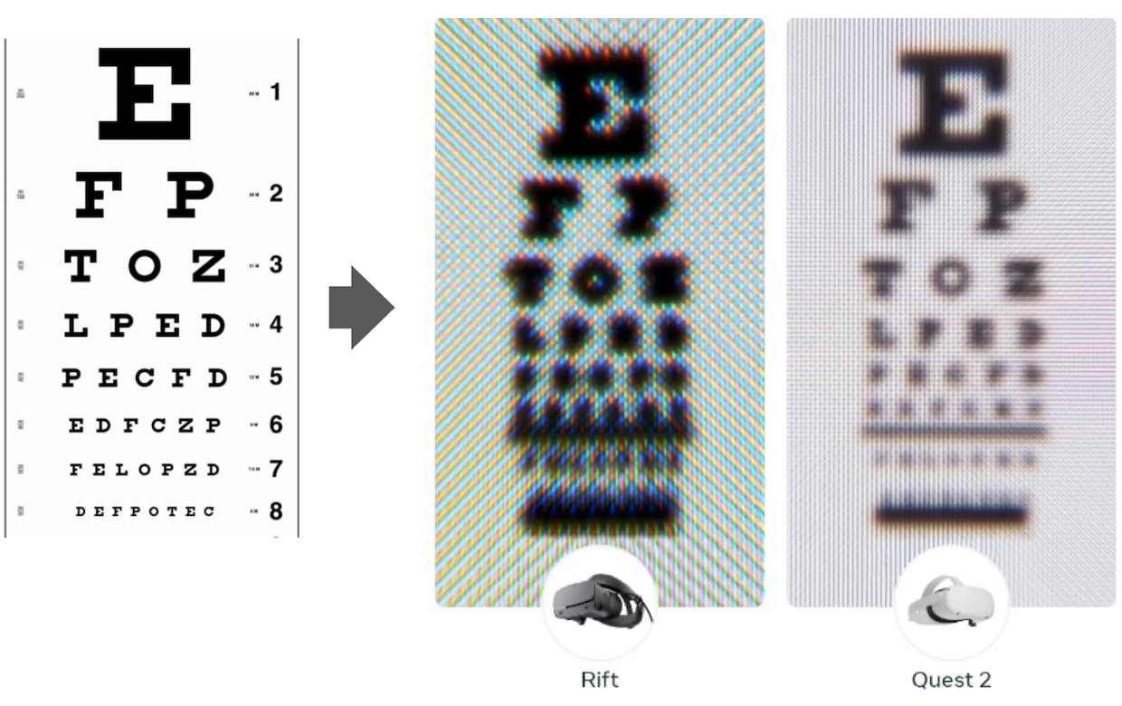
Two reasons prevent current AR/VR devices from achieving truly “indistinguishable from reality” levels. First, to be indistinguishable at the human retinal level requires at least 8,000 PPI (Pixels Per Inch) and 20,000 nits of brightness. However, current LCD (Liquid Crystal Display) and OLED (Organic Light-Emitting Diode) technologies remain at 3,000-4,000 PPI and below 10,000 nits. Second, they cannot reproduce the same dynamic range (brightness-to-darkness spectrum) as the natural world—such as the sparkle of light reflecting off windows or fireworks and explosions in darkness.
Micro-LED technology holds the key to solving these challenges. LCDs and OLEDs generate and convert light through backlights and color filters, resulting in poor energy efficiency and limited brightness. In contrast, micro-LEDs use a “self-emissive” method where each pixel emits its own light, theoretically enabling overwhelming specs of 20,000 PPI and one million nits. However, the absence of red micro-LEDs has prevented commercialization.
Apple Vision Pro boasts the highest specs among AR/VR devices currently on the market. Equipped with micro-OLED displays exceeding 4K resolution, it achieves approximately 3,000 PPI. However, priced at $3,499 (599,800 yen in Japan), it still hasn’t reached the “indistinguishable from reality” level. Meta’s Quest 3 adopts LCD to achieve a more affordable price point but falls short of Apple Vision Pro in resolution and brightness.
If micro-LED technology becomes practical, it could enable performance far exceeding these devices at lower cost. But to do so requires solving the red color challenge. IntraPhoton holds the innovative solution to this problem.
The “Intra-Center Luminescence” Breakthrough
IntraPhoton’s core technology is based on an entirely new light-emission principle called “intra-center luminescence,” developed by Professor Fujiwara. He teaches at Ritsumeikan University’s Research Organization of Science and Technology and is an internationally recognized researcher in semiconductor engineering, particularly nitride semiconductors (GaN-based materials).
Intra-center luminescence technology is realized by introducing (doping) europium (Eu), a rare earth element, into gallium nitride (GaN), the standard LED material. Conventional red LEDs use a material called indium gallium aluminum phosphide (InGaAlP), but this material has a fatal flaw: luminous efficiency drops sharply as element size decreases, becoming essentially unusable below 10 micrometers.
This phenomenon, called the “size effect,” occurs because in InGaAlP materials, surface defects significantly impact luminous efficiency. As elements become smaller, the ratio of surface area to volume increases, and the influence of surface defects grows proportionally, reducing luminous efficiency.
Professor Fujiwara’s technology is revolutionary in fundamentally solving this problem. In GaN material doped with europium, the light-emission mechanism is completely different from conventional approaches. Red light is emitted through 4f inner-shell transitions within europium atoms (optical electronic transitions that occur in rare earth element ions, which appear as emission spectra that are minimally affected by external environmental conditions), making it almost unaffected by the crystal’s surface conditions. In other words, luminous efficiency remains constant regardless of miniaturization.
This new material’s three decisive advantages overturn industry conventions:
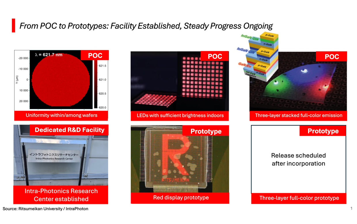
- Size-independent luminous efficiency: Conventional red LED materials suffer dramatic efficiency degradation when they reach sizes below 10 micrometers. However, IntraPhoton’s technology maintains full red luminous efficiency even when miniaturized to 5 micrometers or 3 micrometers (equivalent to 8,000 PPI). This characteristic has already been verified through research and development supported by JST’s Deep Tech Startup International Development Program (D-Global), a government-backed initiative providing 300 million yen (approximately $2 million USD) over three years to bridge university research and commercialization.
D-Global is a program supporting research and development projects aiming for entrepreneurship and commercialization based on university research results. Specializing in “bridging research” for practical application of technology seeds, it plays a role in filling the gap between academic research results and business. Ritsumeikan University has received support from this program since April 2024 and is advancing technology demonstration and commercialization preparation over three years until March 2027. - High wavelength uniformity within and between wafers: With conventional technology, when growing LED crystals on silicon wafers, emission wavelengths vary between the wafer’s center and edges, making products unusable. Additionally, wavelengths differ between multiple wafers made under identical manufacturing conditions, resulting in extremely poor yields.
IntraPhoton’s material maintains identical wavelengths everywhere without any variation. This occurs because intra-center luminescence happens through 4f inner-shell transitions in europium atoms, remaining almost unaffected by external fields. This high uniformity directly leads to improved yields during mass production, becoming a crucial element in cost reduction. - Dramatic manufacturing cost reduction: Since red uses the same gallium nitride material as blue and green, all three colors can be stacked on a semiconductor wafer and directly micro-processed into light-emitting elements at the micrometer level. This eliminates the high-cost process of separately cutting red, blue, and green elements, sorting them, and rearranging them.
In conventional micro-LED display manufacturing, a process called “mass transfer” has been a major bottleneck. Cutting red, blue, and green LED chips made from different materials into micrometer-scale tiny sizes, selecting good products, and placing them in precise positions is technically extremely difficult, time-consuming, and enormously expensive.
With IntraPhoton’s technology, all colors form on the same GaN substrate, enabling batch micro-processing using standard photolithography techniques from semiconductor manufacturing. This means mature semiconductor manufacturing technology can be directly utilized, making the path to mass production clear.
Professor Fujiwara’s research actually began over 10 years ago. Initially aimed at developing a new type of red LED from the beginning, he recognized the potential for micro-display applications as demand for AR/VR devices grew. Multiple academic papers have been published and attracted attention at international conferences. However, commercializing the technology and bringing products to market required business expertise. The encounter with Honkura became the catalyst for IntraPhoton’s birth.
Adopting Semiconductor Economics for Display Manufacturing
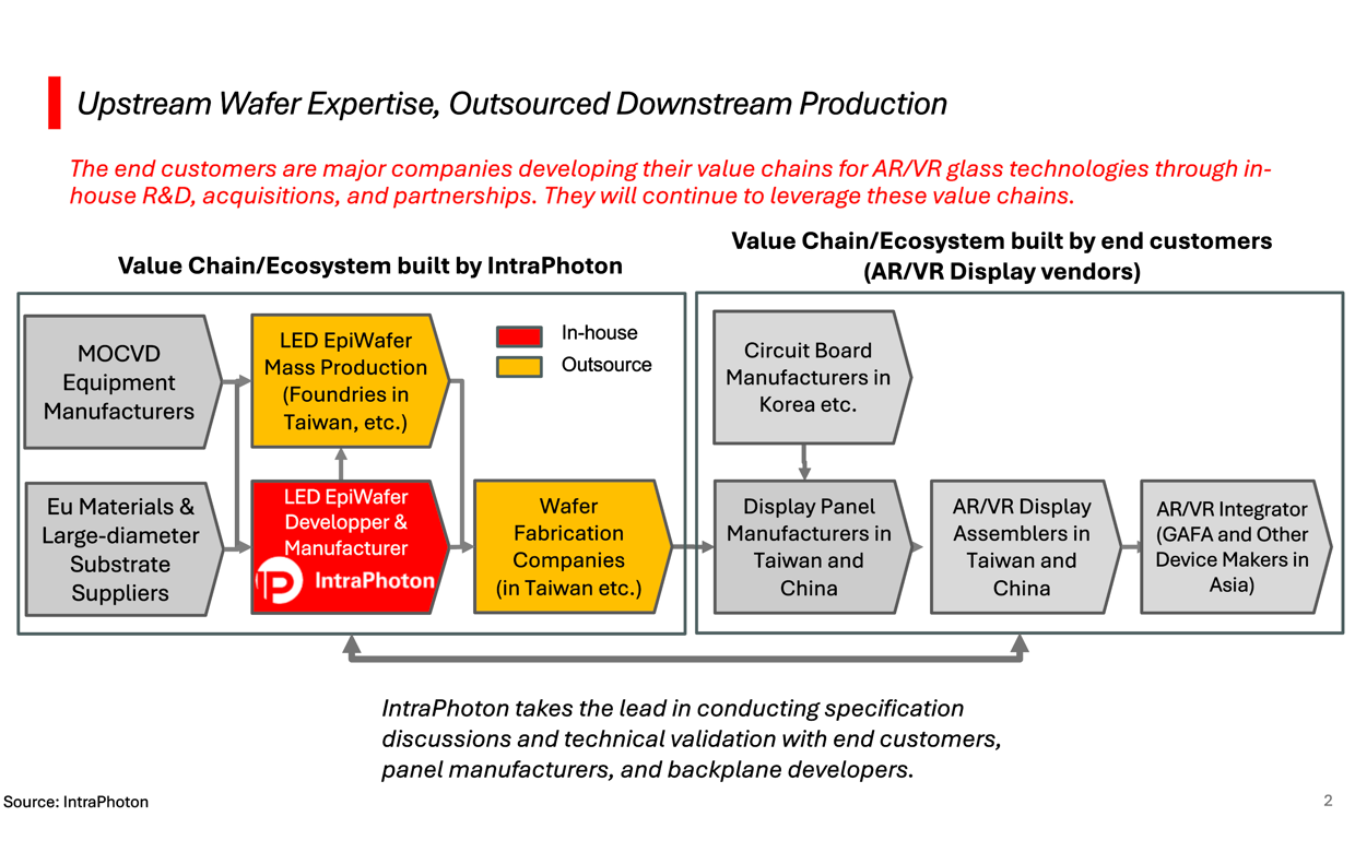
IntraPhoton’s business model differs fundamentally from traditional display industries. Rather than the vertically integrated model adopted by Korean companies like Samsung and LG—fully integrating from upstream to downstream and competing through massive capital investment—it adopts the fabless-foundry model of the semiconductor industry.
The history of Japanese companies struggling in the display industry is well known. Sharp, Sony, Panasonic and others once made huge investments in display businesses but were forced to withdraw or downsize one after another, defeated in price competition with Korean and Chinese companies. The main reason was that display manufacturing is a “capital-intensive industry” requiring continuous investment in large-scale factories. Samsung and LG, with national support, made equipment investments at levels competitors couldn’t match, achieving economies of scale.
“The biggest reason Japanese display makers lost was getting drawn into capital investment competition. Building factories, then next-generation factories, then even larger factories—Japanese companies couldn’t win that competition against Korean and Chinese companies with superior capital. So we decided not to compete on that playing field. (Honkura)
IntraPhoton won’t compete on that playing field. The company’s approach more closely resembles the business models of semiconductor companies like TSMC (Taiwan Semiconductor Manufacturing Company), NVIDIA, and Rapidus.
From a display industry perspective, displays mean doing everything from start to finish—LG does it all, Samsung does it all—that’s the vertically integrated model. It’s not a semiconductor way of thinking. But what we’re doing is completely semiconductor-based, so it becomes very similar to business models like Rapidus and TSMC. (Honkura)
Specifically, IntraPhoton specializes in micro-LED element design and critical manufacturing processes, outsourcing actual manufacturing to partner companies. It cooperates with crystal growth equipment makers on joint development and optimization, outsources mass production to Taiwanese foundries, develops backplanes (circuit boards driving light-emitting elements) with Korean companies, and leaves final display assembly and integration to customer companies.
This approach allows IntraPhoton to concentrate management resources on technology development and intellectual property while avoiding massive capital investment. It also benefits from large-diameter expansion in semiconductor manufacturing (wafer size enlargement). Currently conducting R&D with 2-inch wafers, the company plans to scale up to 6-inch and eventually 12-inch wafers, dramatically increasing the number of displays obtainable per wafer and reducing unit costs.
Why does larger wafer diameter lead to cost reduction? Comparing a 2-inch (approximately 5cm diameter) wafer with a 12-inch (approximately 30cm diameter) wafer shows roughly 36 times the area. Meanwhile, manufacturing costs don’t vary greatly with wafer size. Crystal growth and micro-processing processes take roughly the same time, equipment, and material costs regardless of wafer size. In other words, larger diameters dramatically increase products per wafer, drastically lowering cost per product.
Currently we’re doing R&D with 2-inch wafers, but for mass production we’ll use 12-inch wafers. With 36 times the area, you get 36 times the products at roughly the same manufacturing cost. Simple calculation makes cost 1/36th. That’s the power of the semiconductor model. (Honkura)
The “product” that can be manufactured with IntraPhoton’s LED technology is an ultra-small display measuring approximately 2mm × 1mm—smaller than a grain of rice, yet packed with 8,000 PPI equivalent high resolution. A 12-inch wafer yields thousands of these tiny displays.
The semiconductor industry employs two approaches to reduce per-chip costs: wafer diameter enlargement and chip miniaturization. In the CPU and GPU world, TSMC and Samsung compete in extreme miniaturization technologies at 3 nanometers and 2 nanometers. In Japan, Rapidus is building a factory in Hokkaido targeting 2-nanometer generation semiconductor manufacturing.
For IntraPhoton, display element miniaturization is necessary but doesn’t require CPU-level extreme miniaturization. The micrometer level (1000 nanometers)—adequately handled by current semiconductor technology—suffices. This represents a major advantage. Cutting-edge miniaturization technology involves enormous development and manufacturing costs, but IntraPhoton can leverage mature technology to control costs.
In the semiconductor world, extreme miniaturization competition at 2 and 3 nanometers is unfolding, but micrometer level suffices for us. In other words, we can use already established mature technology, so both development risk and costs are dramatically reduced. (Honkura)
Target markets are clear. Market research companies predict the micro-LED AR/VR display market will grow to approximately 500 billion yen (about $3.3 billion USD) by 2032. The LED element sales market alone represents about 75 billion yen (approximately $500 million USD). IntraPhoton aims to capture significant market share backed by technological superiority.
Furthermore, future expansion into broader applications is envisioned—wearable devices like Apple Watch, vehicle displays in Teslas, and even large TVs. Total market scale is predicted to exceed one trillion yen (approximately $6.7 billion USD).
Milestones Already Achieved
IntraPhoton’s technology development is progressing at remarkable speed. JST’s D-Global program began in April 2024, targeting achievement of 8,000 PPI and 20,000 nits over three years until March 2027. However, as of October 2025—the program’s midpoint—8,000 PPI is already proven.
We’ve demonstrated that it lights up even at 3 micrometers, and we’ve achieved about 10,000 nits of this target 20,000-nit brightness with red alone. When we light up all three colors—red, blue, green—in full color, brightness roughly triples to about 30,000 nits. In other words, we have six times the brightness of Apple Vision Pro and have achieved roughly double the resolution—that’s our current position. (Honkura)
Three micrometers corresponds to 8,000 PPI. Having 8,000 pixels in one inch (2.54 centimeters) means pixel spacing of approximately 3 micrometers. Considering human hair diameter ranges from 50-100 micrometers, this represents astonishing fineness at less than 1/20th that size.
The 30,000-nit figure is also astonishing. Typical indoor lighting brightness is several hundred lux, while sunny outdoor conditions reach 100,000 lux. Though units differ from the nit (cd/m²) used for display brightness, preventing direct comparison, 30,000 nits is extremely bright—visible even under direct sunlight. Considering Apple Vision Pro’s approximately 5,000 nits is considered industry-leading, six times that at 30,000 nits demonstrates how revolutionary this is.
Within Ritsumeikan University, a dedicated R&D facility with cleanroom called the “Intraphotonics Research Center” has been established. Cleanrooms are ultra-clean manufacturing environments with airborne dust and particles removed to the extreme—essential for semiconductor and display manufacturing. When handling elements just a few micrometers in size, even minute dust particles cause product defects, requiring strict management.
Ritsumeikan University’s support played a crucial role in establishing this cleanroom. The university supports pre-incorporation research and development through its RIMIX commercialization support program. RIMIX is a support system aimed at accelerating social implementation of Ritsumeikan University research results, providing funding and facilities needed for laboratory-level commercialization preparation. Universities providing dedicated research facilities for startups remains rare in Japan, demonstrating IntraPhoton and Ritsumeikan University’s strong commitment.
Prototype development is also steadily progressing. Red LEDs have already been driven as displays, successfully demonstrating the display of Ritsumeikan University and IntraPhoton logos. This represents an important milestone showing not just individual LED elements lighting up, but controlling them to display arbitrary images.
The next step is creating full-color (red, blue, green) demonstration displays. Wafers with stacked red, blue, and green layers have already been fabricated and light emission confirmed. Driving these as actual displays requires bonding with backplanes (drive circuits). Currently, this is being developed in cooperation with domestic companies, but in the future, this process is planned to be advanced in cooperation with specialized companies in Europe and Korea.
Ecosystem building proceeds in parallel with technical progress. With crystal growth equipment makers, equipment improvement optimized for IntraPhoton’s special materials is underway. With Taiwanese foundry companies, initial discussions toward mass production have begun. Korean backplane manufacturers have also begun initial discussions about circuit design matching IntraPhoton’s element specifications.
For biotech companies, there’s a relatively simple path—having products and excellent clinical data leads to acquisition by major companies. But our business isn’t like that. Equipment makers, foundries, backplane manufacturers, final product makers—many players are intricately intertwined, so strategically designing business development regarding who to partner with, when, and how to distribute profits is extremely difficult. (Honkura)
The micro-LED industry hasn’t matured yet. Each player is groping forward with technology development and business model construction. Therefore, building relationships with key players early and occupying central positions in the ecosystem becomes crucial. IntraPhoton is advancing this positioning leveraging technological superiority.
The Entrepreneur-Academia Partnership
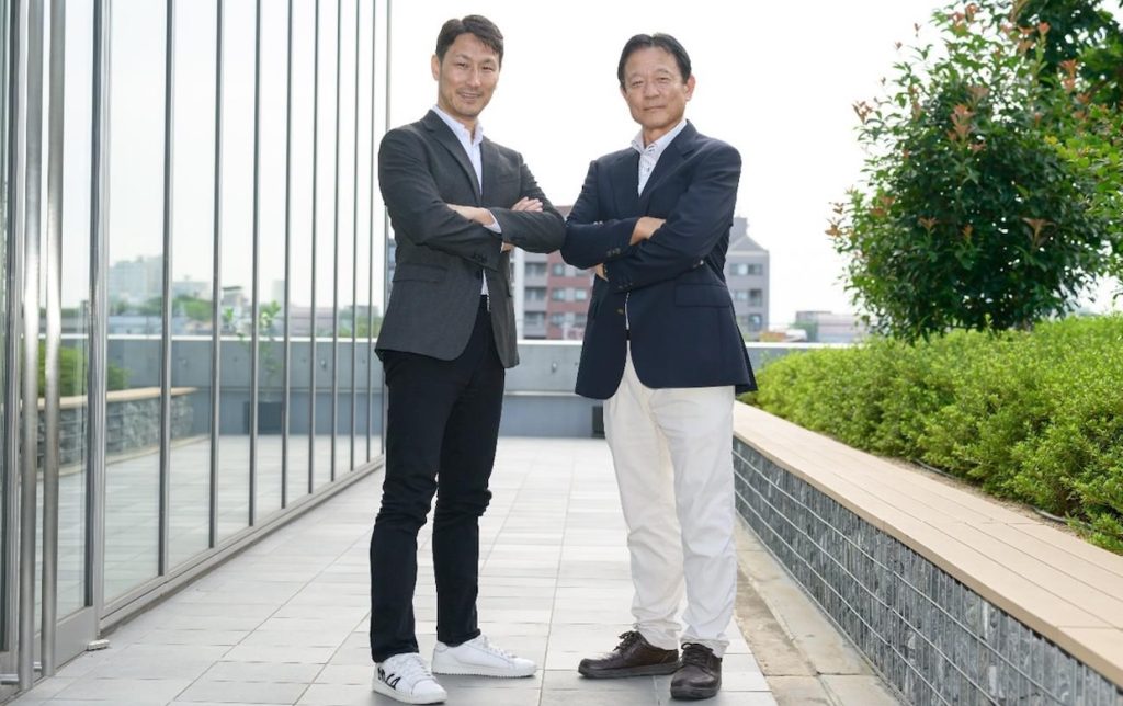
Photo credit: IntraPhoton
Behind IntraPhoton’s birth lies a considerable preparation period between Toshihiko Honkura and Professor Yasufumi Fujiwara. The two met in 2022 through an introduction from Osaka University’s industry-academia collaboration division.
Honkura’s career started as a researcher at the University of Tokyo. During that period, international competition in the Human Genome Project was intensifying, with US startup Celera Genomics attempting to overtake in just a few years what research institutions worldwide had spent decades pursuing—the human genome sequencing. Witnessing this competition, Honkura developed strong interest in startup potential.
Subsequently, feeling his aptitude lay more in bridging science and business than pursuing a narrow research field, Honkura transitioned to securities analyst. During that period, Japanese bio-ventures were going public in succession—he covered companies like AnGes and OncoTherapy Science. After management consulting at McKinsey, he experienced startup investment at the Innovation Network Corporation of Japan (now Industrial Innovation Investment Corporation). Then in 2013, he founded Osaka University spinout Quantum Biosystems.
When I started my previous company in 2013, support systems for Japanese startups aiming for global expansion weren’t established. Since we were targeting world markets from the start, after a large fundraising round, we brought Osaka University technology to Silicon Valley, built an organization locally, and began operations.
We advanced technology development partnering with major US semiconductor companies, but ultimately didn’t achieve commercialization. In 2021, after transferring some business results and intellectual property rights to a major US corporation, we dissolved the company. However, this experience provided important lessons about global expansion. (Honkura)
This experience brought Honkura important lessons: For global expansion, technical excellence alone is insufficient—business sustainability, market positioning, appropriate business model design, and diverse organizations that enable these are essential.
After the business transfer, Honkura joined i-nest Capital as a partner, supporting global expansion of Japanese deep-tech startups. While residing in Austin, Texas, he provided comprehensive support for Japanese companies expanding into the US market—visa acquisition, patent applications, office establishment, recruitment, and partnerships with local companies.
In 2022, while Honkura was back in Japan for i-nest Capital business, Osaka University’s industry-academia collaboration division introduced him to Professor Yasufumi Fujiwara, who was then at Osaka University. Since Honkura’s previous startup was an Osaka University spinout, he maintained continuous relationships with Osaka University’s industry-academia collaboration staff. Professor Fujiwara already desired startup establishment but lacked a clear vision for commercialization direction. He had approached business companies and VCs but failed to find directions leveraging the technology’s true value.
I proposed to Professor Fujiwara: if you want to establish a company, the establishment itself is easy for anyone. If the goal is just announcing a startup’s creation, that’s simple. But if you truly want to maximize this invention’s value, the story differs. There’s a very large market, and this technology must go global from the start.
However, at that time, I myself didn’t have deep knowledge about the AR/VR market. So I proposed: within the scope of what I can do as an individual, why don’t we explore business possibilities together, thinking only about growing globally. (Honkura)
From there, Honkura and Professor Fujiwara refined the business plan together. They attended international conferences, engaged with global players, and initiated preliminary dialogues with AR/VR device makers as potential customers. Then Professor Fujiwara applied to JST’s D-Global program and, with advice and support organization introductions from Honkura, won selection.
A support organization that played an important role in the selection was Beyond Next Ventures, whose CEO Tsuyoshi Ito was also the first investor in Honkura’s previous startup Quantum Biosystems.
IntraPhoton’s advisory board includes top-class industry experts. Hidenori Kawanishi led the micro-display business at Sharp using quantum dot (QD) color conversion technology. Takao Nakamura led the epi-wafer manufacturing and sales business at Sumitomo Electric Industries and has extensive experience in this business.
IntraPhoton’s global strategy isn’t merely exporting products. It’s a strategy to build the manufacturing ecosystem itself globally. Crystal growth in Japan or Taiwan, wafer processing at Taiwanese foundries, backplanes in Korea, final assembly at customer companies (mainly in the US)——the company presupposes an international division of labor.
Furthermore, the recent America First manufacturing domestic return policy could present opportunities for IntraPhoton. The CHIPS and Science Act, enacted under the Biden administration, strongly promotes attracting semiconductor manufacturing to the US. TSMC is building large-scale factories in Arizona, and Samsung is expanding factories in Texas.
The US is advancing manufacturing domestic return. Movement to attract semiconductor and display factories to regions like Arizona, Phoenix, and Texas is becoming active. In Korea, hundreds of billions of yen in subsidies are being provided specifically for the micro-LED field. Unfortunately, in Japan, there are almost no such movements in the display and LED fields, so building manufacturing ecosystems overseas from the start is essential for us.
In terms of entering such global manufacturing communities, I believe continuously disseminating information through media is important. By regularly announcing technology development progress, corporate partnerships, milestone achievements, we want to enhance our presence within the industry. (Honkura)
If manufacturing bases are established in the US, IntraPhoton envisions production there. For US companies like Apple, Meta, and Google——the customers——supply chain security is an important consideration, and US domestic manufacturing capability becomes a major advantage.
Looking Toward Post-2027 Growth
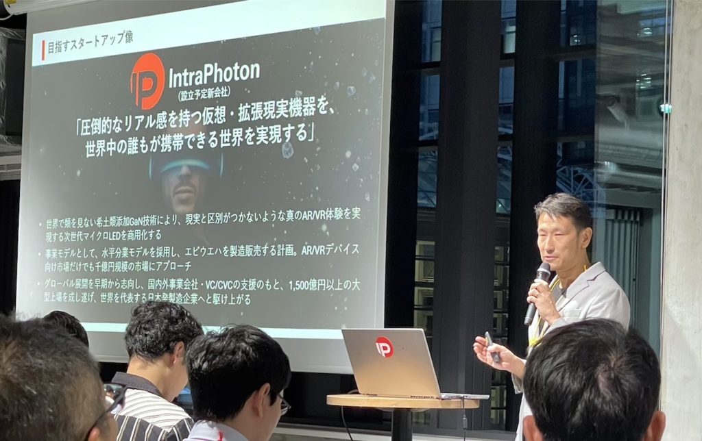
Photo credit: Growthstock Pulse
IntraPhoton’s fundraising strategy is carefully and strategically designed. Currently, the company advances incorporation and initial R&D combining multiple grant and support programs.
The core is JST’s D-Global program (offering 300 million yen as a grant, approximately $2 million USD, over three years). This is a grant specialized for R&D, allocated to technology demonstration and prototype development. During the period from April 2024 to March 2027, the company aims to achieve 8,000 PPI and 20,000 nits, and develop full-color prototypes.
D-Global is limited to R&D funding and cannot be used for incorporation costs, initial personnel expenses, marketing expenses, etc. Filling this gap are UTokyo IPC’s 1stRound program (offering up to 5 million yen as a grant, approximately $33,000 USD) and Ritsumeikan University’s RIMIX program.
IntraPhoton plans its full-scale seed round for April 2027—immediately after D-Global ends. The seed round envisions raising 300-500 million yen (approximately $2-3.3 million USD). Furthermore, applications to grant programs such as NEDO (New Energy and Industrial Technology Development Organization) are also planned.
From 2027 to 2029 will be a period for prototype refinement and concrete discussions with initial customers. During this time, full-scale business negotiations with target customer companies like Apple, Meta, and Google are expected to begin. Initial dialogues have already started, and high interest in technical possibilities has been expressed.
In 2029, initial product market introduction is planned. This “first generation” product will exceed current AR/VR devices in resolution and brightness but won’t reach final target specs. However, it will have sufficient performance for specific applications and early adopters.
And in the early 2030s, “second generation” products will be introduced. At this stage, the company aims to achieve truly “indistinguishable from reality” performance levels and win adoption in mainstream products of at least one GAFAM company.
Assuming the second-generation product launches and gets adopted by even one GAFAM company, we’re looking at about 16 billion yen (approximately $107 million USD) in sales, with operating profit around 5.6 billion yen (approximately $37 million USD). With a PER of 50 times for startup valuation, market capitalization would be about 160 billion yen (approximately $1.1 billion USD). However, these are very conservative numbers, and listing isn’t limited to Japan—NASDAQ is also an option. We’re aiming for a listing in the hundreds of billions of yen scale. (Honkura)
The micro-LED display market is predicted to grow rapidly, with companies achieving technological breakthroughs potentially monopolizing the market. Looking at the semiconductor industry, NVIDIA dominated the AI GPU market and reached a market capitalization of several trillion dollars. IntraPhoton’s target scale of hundreds of billions of yen is fully achievable with global market success.
The period until the planned 2027 fundraising is also a time to focus on customer development and partnership building. Participating in global conferences, disseminating IntraPhoton’s technology, deepening dialogue with potential customers and partner companies, raising awareness through media—these activities become the foundation for full-scale business expansion after 2027.
If IntraPhoton’s “indistinguishable from reality display” is realized, it won’t be mere gadget evolution. According to a 2023 McKinsey & Company technology trends survey, “deskless workers”—workers not at desks—comprising about 80% of the global workforce, are predicted to become AR/VR technology’s largest adopters. These are people working in agriculture, construction, healthcare, education, manufacturing, transportation, retail, and hospitality industries. Already 63% of companies have introduced immersive technology for training purposes.
In these industries, people traditionally worked away from information terminals, making real-time access to necessary information difficult. However, if ultra-high-definition, lightweight AR/VR devices are realized, instantly diagnosing crop conditions on farms, viewing 3D blueprints at construction sites, or instantly referencing patient information in medical settings becomes possible.
People working at desks in offices can work while obtaining various information. But in reality, in agriculture, construction, healthcare, and education, very many people work without information terminals. If real information instantly appears before their eyes, indistinguishable from reality, it will greatly change how work is done and how people communicate—becoming an industry with enormous impact. (Honkura)
Combinations with generative AI also hold great potential. Necessary information instantly displayed before your eyes, with AI providing real-time advice. Even people without specialized knowledge can make expert-level judgments. IntraPhoton’s ultra-small displays measuring 2mm × 1mm can be incorporated not just into glasses but any device. Combined with optical systems for magnified display, they can expand into various applications.
We’re starting with small red micro-LEDs, but we’re aiming to become a startup that grows overwhelmingly large from Japan. (Honkura)
On October 6, 2025, a startup was born in Shiga Prefecture. The moment when Japanese-originated technology achieves true global success may arrive in a few years.